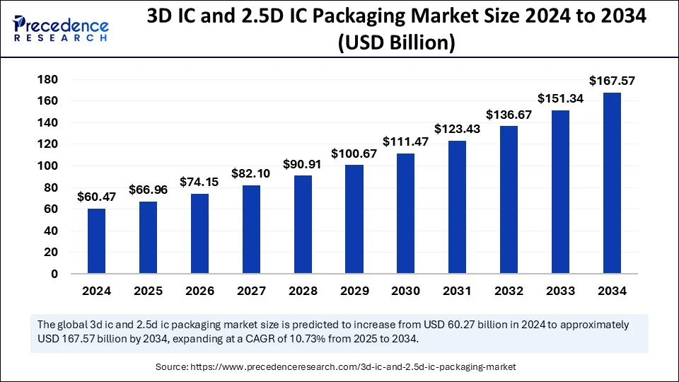
3D IC and 2.5D IC Packaging Market Size to Hit USD 167.57 Bn by 2034

3D IC and 2.5D IC Packaging Market Key Takeaways
- Asia Pacific dominated the 3D IC and 2.5D IC packaging market in 2024.
- North America is expected to witness the fastest growth during the forecast period.
- By packaging technology, the 3D wafer-level-chip-scale packaging (WLCSP) segment captured the biggest market share in 2024.
- By application, the MEMS/Sensors segment held the largest market share in 2024.
- By end use, the consumer electronics segment led the market in 2024.
3D IC and 2.5D IC Packaging Market Overview
The 3D IC packaging consists of the integration of multiple layers or vertical stacking of dies, which helps create a three-dimensional structure. On the other hand, the 2.5D IC packaging is the integration of multiple chips or dies with a silicon interposer or organic substrate. Ongoing advancements in semiconductor packaging technologies are one of the key factors boosting the growth of the 3D IC and 2.5D IC packaging market.
These packaging solutions are easy to integrate into the complex and smaller architecture of the electronics devices. There is a rising demand for consumer electronics, which is boosting the growth of this market. In addition, the rising government initiatives to boost the production of semiconductors directly impact this market’s growth.
3D IC and 2.5D IC Packaging Market Drivers
One of the key drivers of this market is the exponential growth of data-intensive applications such as AI, IoT, autonomous vehicles, and high-performance computing. These applications require faster processing speeds and higher data throughput, which traditional planar ICs cannot accommodate efficiently.
Another major driver is the miniaturization trend in electronics, particularly in smartphones, wearable devices, and medical implants. 3D IC and 2.5D IC packaging technologies offer space-saving solutions by stacking chips vertically or combining them on a single substrate, optimizing size and functionality. The demand for high-bandwidth memory (HBM) and energy-efficient data centers is further propelling market growth.
3D IC and 2.5D IC Packaging Market Opportunities
The evolving market landscape presents abundant opportunities for players involved in interposer design, through-silicon via (TSV) fabrication, and die stacking. The rise of chiplet-based architectures is expected to create a new wave of demand for heterogeneous integration, where different functional units can be manufactured independently and later assembled into a unified package using 2.5D or 3D techniques.
There is also growing interest in integrating different nodes of technology (such as logic and memory) within the same package, which opens opportunities for collaboration between foundries, OSATs, and design houses. Furthermore, innovations in thermal management and power delivery systems within 3D structures can offer competitive advantages.
3D IC and 2.5D IC Packaging Market Challenges
Despite their benefits, 3D and 2.5D IC packaging technologies face a range of technical and manufacturing challenges. Yield loss during TSV integration and die stacking remains a concern, as does the complexity of testing and validating the final package. Thermal dissipation is a critical issue in 3D ICs due to the close proximity of heat-generating components.
The high cost of implementation, specialized equipment requirements, and longer development cycles are additional hurdles for widespread adoption. Additionally, ensuring reliability and long-term performance across vertically stacked dies demands sophisticated engineering solutions.
3D IC and 2.5D IC Packaging Market Regional Insights
North America leads the market, driven by robust R&D activities and the presence of semiconductor giants engaged in high-end packaging. The U.S. in particular is home to companies heavily investing in AI, data centers, and defense electronics, all of which are key applications for 3D ICs. Asia Pacific is growing rapidly, led by Taiwan, South Korea, and China.
Taiwan’s foundries and OSAT players are among the pioneers in 2.5D IC implementation. South Korea’s dominance in the memory market and China’s focus on semiconductor self-reliance are fueling demand. Europe remains a critical player in automotive and industrial IoT applications where advanced packaging is gaining relevance.
3D IC and 2.5D IC Packaging Market Recent Developments
In recent years, several major players have announced breakthroughs in 3D packaging processes. The development of hybrid bonding and wafer-to-wafer stacking techniques is becoming more mainstream. Companies like TSMC, Intel, and Samsung are actively pursuing next-gen packaging roadmaps involving 3D SoC and advanced interposers.
TSMC’s CoWoS and SoIC technologies and Intel’s Foveros are setting industry standards. There is also an increase in partnerships between fabless companies and OSAT providers to fast-track integration of these advanced packaging methods into commercial products.
3D IC and 2.5D IC Packaging Market Companies
- Samsung
- Taiwan Semiconductor Manufacturing Company, Ltd. (TSMC)
- Intel Corporation
- ASE Technology Holding Co., Ltd.
- Amkor Technology
- Broadcom
- Texas Instruments Inc.
- United Microelectronics Corporation (UMC)
- JCET Group Co., Ltd.
- Powertech Technology Inc.
Segments Covered in the Report
By Packaging Technology
- 3D Wafer-Level Chip-Scale Packaging (WLCSP)
- 3D Through-Silicon Via (TSV)
- 2.5D
By Application
- MEMS/Sensors
- Logic
- Imaging & Optoelectronics
- Memory
- LED
- Others (Power, Analog & Mixed Signals, RF, Photonics)
By End Use
- Consumer Electronics
- Industrial
- Telecommunications
- Automotive
- Military & Aerospace
- Medical Devices
By Region
- Asia Pacific
- North America
- Europe
- Latin America
- Middle East and Africa (MEA)
Ready for more? Dive into the full experience on our website!
